

Dutch lithography machine maker ASML lately dethroned Utilized Supplies to grow to be the world’s largest fab device maker, and its future appears even brighter following information that it’s ramping up manufacturing of its new Excessive-NA (numerical aperture) EUV (excessive ultraviolet) machine.
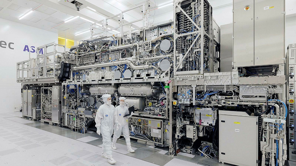
This method, which is the scale of a double-decker bus and weighs 150,000 kg, is able to etching traces simply 8 nm huge on semiconductors. It is a important discount in comparison with the earlier era, permitting extra transistors to be packed on a chip, resulting in sooner processing and better storage capability, which is important for AI functions.
Intel, a significant buyer, has already obtained its first machine at its D1X manufacturing unit in Oregon and plans to start manufacturing utilizing the system by the tip of 2025.
Not for China
“Intel’s focus is to stay on the forefront of semiconductor lithography expertise, and we now have constructed our EUV experience and capabilities over the previous 12 months. Working carefully with ASML, we are going to leverage Excessive-NA EUV’s high-resolution patterns as one of many methods we proceed Moore’s Legislation and keep our robust historical past of development right down to the smallest of geometries,” mentioned Dr. Ann Kelleher, government vp and normal supervisor of expertise growth at Intel.
ASML says it has taken between 10 and 20 orders up to now for its machine, which is priced at a whopping $350 million, indicating optimistic expectations for the expertise. This comes regardless of allegations in regards to the cost-effectiveness of next-generation lithography instruments for upcoming nodes.
Though China was ASML’s second-largest market final 12 months, Reuters experiences that the brand new gadget won’t be offered to producers there after the US authorities cracked down on exports of superior expertise to the Individuals’s Republic.
EUV lithography, distinctive to ASML, prints microchips utilizing gentle with a wavelength of solely 13.5 nm – close to X-ray vary. ASML (and Intel) say the expertise is driving Moore’s Legislation ahead and supporting new transistor designs and chip architectures.
The brand new platform is predicted to assist high-volume chip manufacturing by 2025-2026, enabling geometric chip scaling into the following decade. By decreasing the variety of course of steps in high-volume manufacturing, chip producers can profit from important reductions in defects, prices and cycle time.